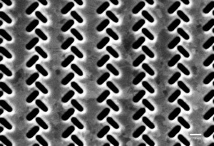
An electron micrograph shows the nanoscale perforations at the surface of the plasmonic coupler. Credit: Jiao Lin and Balthasar Müller.
(Phys.org) —A Harvard-led team of researchers has created a new type of nanoscale device that converts an optical signal into waves that travel along a metal surface. Significantly, the device can recognize specific kinds of polarized light and accordingly send the signal in one direction or another.
Read more at: http://phys.org/news/2013-04-physicists-left-solution-on-chip-optics.html
Pretty important stuff, ducting light around on chips is an important ability for future electronics…or maybe one should say, nano- electro- optic- systems. Cool stuff…
